Little Known Questions About Basic principles of image sensors - CCD working.
from web site
How Fast CCD - Advanced Photon Source can Save You Time, Stress, and Money.
The gate oxide, i. e. the capacitor dielectric, is grown on top of the epitaxial layer and substrate. Later while doing so, polysilicon gates are deposited by chemical vapor deposition, patterned with photolithography, and etched in such a way that the independently phased gates lie perpendicular to the channels. The channels are even more defined by usage of the LOCOS procedure to produce the channel stop area.

These channel stops are produced prior to the polysilicon gates are, as the LOCOS procedure makes use of a high-temperature step that would ruin eviction material. The channel stops are parallel to, and exclusive of, the channel, or "charge bring", areas. Channel stops frequently have a p+ doped area underlying them, supplying a more barrier to the electrons in the charge packages (this conversation of the physics of CCD gadgets assumes an electron transfer gadget, though hole transfer is possible).
This will trigger the CCD to diminish, near the pn junction and will collect and move the charge packets below the gatesand within the channelsof the device. CCD manufacturing and operation can be optimized for various usages. The above process describes a frame transfer CCD. While CCDs may be manufactured on a greatly drugged p++ wafer it is also possible to produce a device inside p-wells that have been positioned on an n-wafer.

The 4-Minute Rule for DISR's CCD detector - The Planetary Society
This method of manufacture is used in the construction of interline-transfer devices. Another variation of CCD is called a peristaltic CCD. In a peristaltic charge-coupled gadget, the charge-packet transfer operation is analogous to the peristaltic contraction and dilation of the digestion system. The peristaltic CCD has an additional implant that keeps the charge away from the silicon/silicon dioxide user interface and creates a big lateral electric field from one gate to the next. Read This [
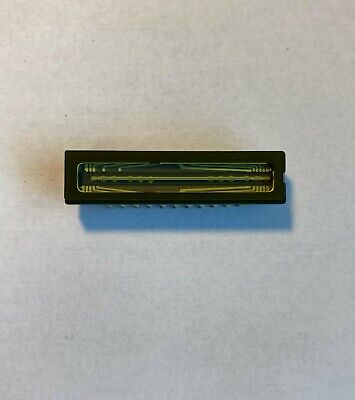
edit] The CCD image sensors can be executed in numerous various architectures. The most common are full-frame, frame-transfer, and interline. The distinguishing attribute of each of these architectures is their technique to the issue of shuttering. In a full-frame device, all of the image area is active, and there is no electronic shutter. The drawback to the frame-transfer.
