How CCD sensors - Vision-Doctor can Save You Time, Stress, and Money.
from web site
Little Known Questions About The CCD Detector - ISDC.
Gadget for the movement of electrical charge A specifically established CCD in a wire-bonded package used for ultraviolet imaging A charge-coupled device (CCD) is an integrated circuit containing a selection of connected, or combined, capacitors. Under the control of an external circuit, each capacitor can transfer its electrical charge to a neighboring capacitor.
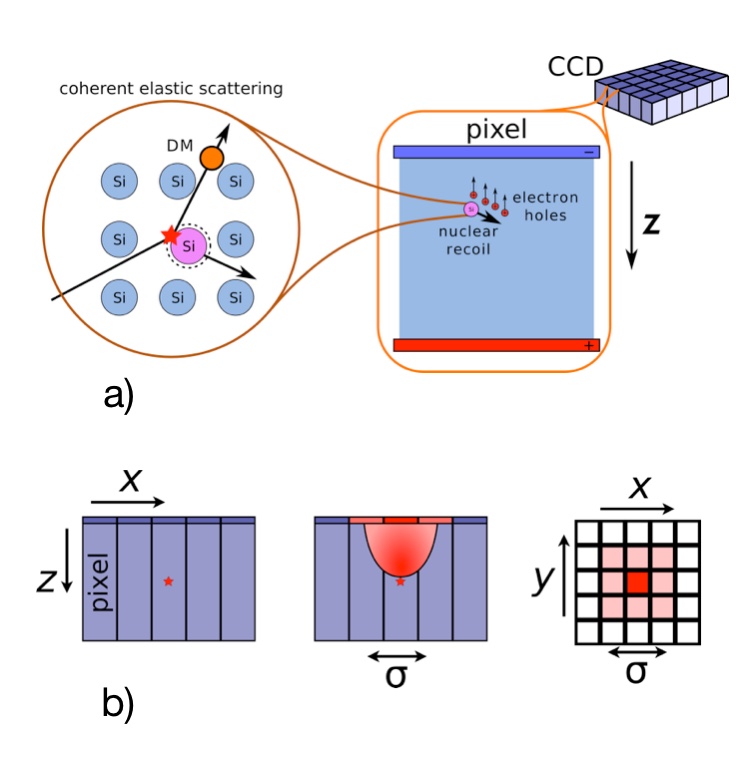
In a CCD image sensor, pixels are represented by p-doped metaloxidesemiconductor (MOS) capacitors. CCD DETECTOR , the basic foundation of a CCD, are biased above the limit for inversion when image acquisition starts, permitting the conversion of incoming photons into electron charges at the semiconductor-oxide user interface; the CCD is then utilized to read out these charges.
Getting My Understanding Binning in High Energy CCD Detectors - Andor To Work
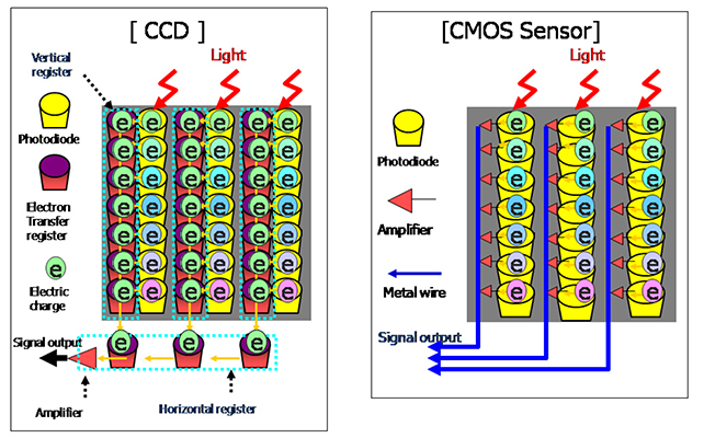
In applications with less exacting quality demands, such as consumer and professional digital cameras, active pixel sensing units, likewise called CMOS sensors (complementary MOS sensing units), are usually used. Nevertheless, the large quality advantage CCDs enjoyed early on has narrowed gradually and because the late 2010s CMOS sensing units are the dominant innovation, having largely if not totally changed CCD image sensing units.
In the late 1960s, Willard Boyle and George E. Smith at Bell Labs were researching MOS innovation while working on semiconductor bubble memory. They understood that an electric charge was the analogy of the magnetic bubble which it might be saved on a tiny MOS capacitor. As it was relatively uncomplicated to fabricate a series of MOS capacitors in a row, they linked a suitable voltage to them so that the charge could be stepped along from one to the next.
Overview of CCD Detectors - Starlink - Truths

They envisaged the design of what they called, in their note pad, "Charge 'Bubble' Devices". The preliminary paper explaining the idea in April 1970 noted possible usages as memory, a delay line, and an imaging device. The device might likewise be used as a shift register. The essence of the style was the capability to move charge along the surface area of a semiconductor from one storage capacitor to the next.
The very first experimental gadget demonstrating the principle was a row of closely spaced metal squares on an oxidized silicon surface area electrically accessed by wire bonds. It was demonstrated by Gil Amelio, Michael Francis Tompsett and George Smith in April 1970. This was the very first speculative application of the CCD in image sensing unit innovation, and used a diminished MOS structure as the photodetector.
